Measurement Sensors
Dimension Measurement
Displacement Measurement
Measurement Sensors for the Semiconductor Industry
Constant pressure to improve the price point of semiconductors has pushed the industry into quickly adopting technologies that drive efficiency. KEYENCE's precision sensors are innovative solutions for inspecting and measuring workpieces and monitoring equipment to help our customers deliver the highest quality semiconductor components at competitive prices. Check out some of the proven solutions below.
Get detailed information on our products by downloading our catalog.
View Catalog![Automated Measurement and Inspection Examples [Semiconductors]](/img/asset/AS_119841_L.jpg)

Importance of Precision Measurements in the Semiconductor Industry
Modern electronics are getting smaller, more powerful and more energy efficient each year. For example, in 2005 the Intel Pentium 4 670 was a single-core CPU with approximately 169 million transistors on its die. For comparison, the Intel Core i9-11900K (released in 2021) is a 10-core CPU with 10.2 billion transistors.
Due to these miniaturizations, lithography manufacturing demands increasingly higher degrees of precision. Advanced measurement sensors are required to ensure precise wafer alignment, increase traceability, and optimize the manufacturing and inspection processes.
We’re here to provide you with more details.
Reach out today!

Wafer Groove Depth (After Etching)
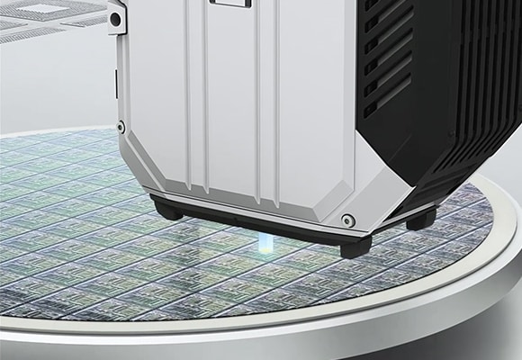
Automate groove depth measurements using the WI-5000 Series. The WI Series can measure mirrored or transparent surfaces without issue. By automating inspection, you can reduce cycle time and avoid common pitfalls of microscope measurements such as human error or inconsistent inspection location.
Wafer Edge Profile Measurement
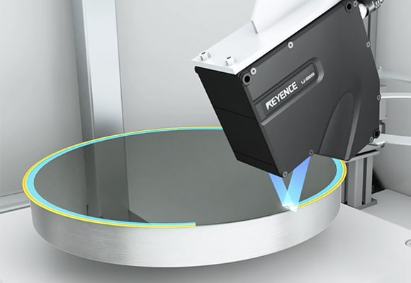
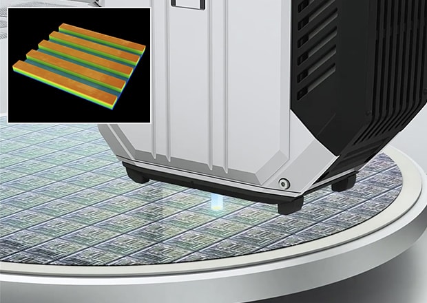
Measure the profile of a wafer edge. By selecting one of the inspection tools such as Height Difference/Width or Angle, users can start measurement easily. The high-resolution image capturing using 3200 points/profile achieves highly accurate profile measurement that was impossible with conventional methods.
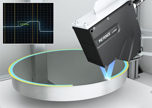
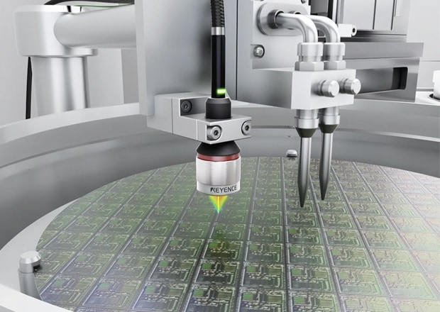
Spin Coating Height Measurement
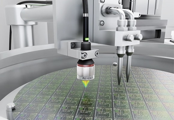
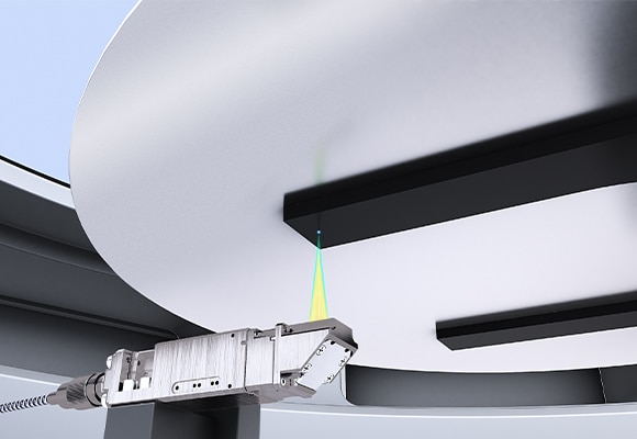
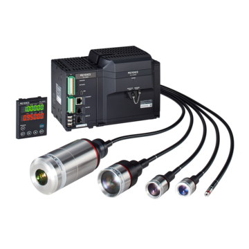
Thanks to the small head size, CL-3000 Series devices can be easily installed on equipment for accurate distance measurement. The sensor can measure both diffuse and mirrored surfaces accurately, without any mounting adjustments.
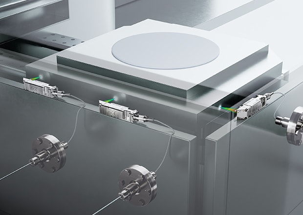
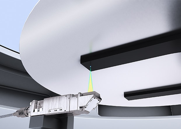
Stage Positioning in Vacuum Environments
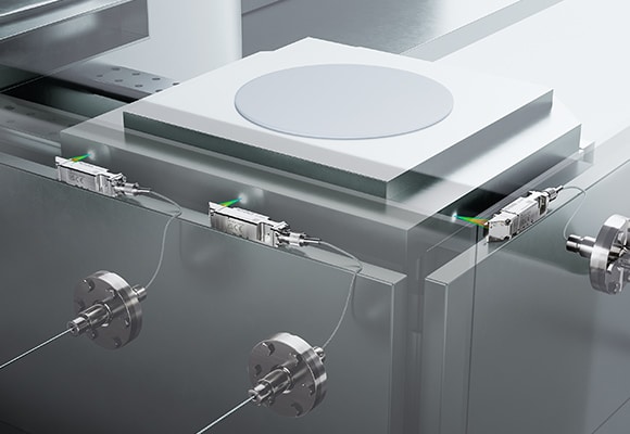
The CL-3000 Series can be used to check the stage home position before processing, and the heat and vacuum resistance also means baking can be performed without having to remove the sensor heads.
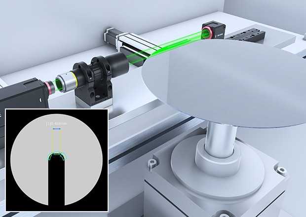
Wafer Edge Shape Measurement
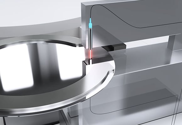
A non-contact measurement is conducted of the wafer edge shape. The TM-X5000 Series with telecentric lens captures the profile in high resolution for accurate measurement.
Robot Arm Height Measurement in Vacuum
Robot arm movement is measured in vacuum conditions. The CL-3000 Series ultra-high vacuum-compatible head can capture device movements that would be impossible to capture in an atmospheric environment. The sensor head is ultra-compact and can be mounted even in areas with limited space.
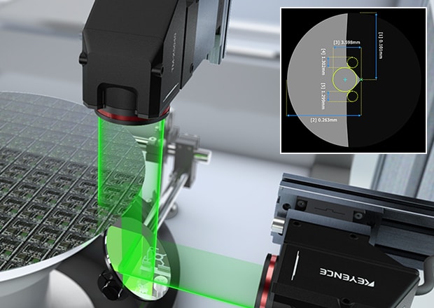
Wafer Notch Position Detection and Dimensional Measurement
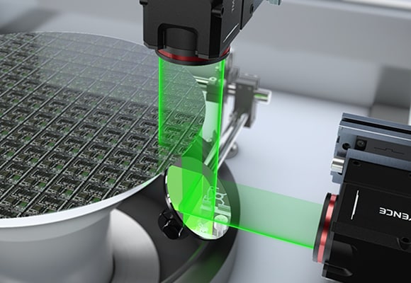
Angled mirrors can be used to perform measurement where installation space is limited. In addition to detecting the coordinates of tangent circles at specified diameters and intersection point coordinates, angled mirrors can also be used to measure notch dimensions and identify shape problems.
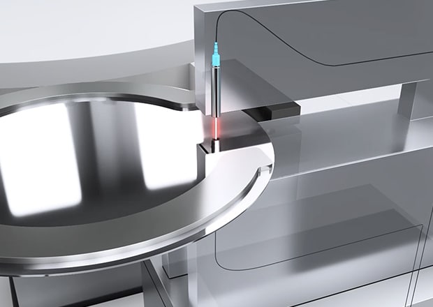
Wafer Thickness After Polishing
Polished wafers need to have an extremely high flatness. The SI-F Series can perform ultra-high precision measurement at a resolution of 0.001 µm. Its optical fiber sensor heads generate no heat, making stable flatness measurement possible.
Semiconductor Component Inspection
The semiconductor industry relies on complex manufacturing steps, which are accompanied by several inspection processes. KEYENCE’s CL-3000 Series confocal laser displacement sensors feature micron level accuracy, and they’re most commonly used to inspect the results of the lapping process as well as the height and uniformity of subsequently added spin coating.
Measuring the groove depth after etching the silicon is crucial to ensure that the etched patterns are of the correct dimensions, and KEYENCE’s WI-5000 Series offers automated groove depth measurement of both mirrored and transparent surfaces while also reducing cycle time, human error, and inconsistent inspection.
Subsequent manufacturing processes in the semiconductor industry include wafer edge profile measurement and finding the wafer notch position for dicing. These inspection steps are typically done with devices such as KEYENCE’s LJ-X8000 Series, which offers 3200 data points per profile.
Semiconductor Equipment Inspection/Monitoring
Precision in the semiconductor industry greatly depends on proper equipment calibration and positioning, which implies occasional inspection and continuous monitoring. KEYENCE’s Spectral-interference laser displacement meter, the SI-F1000 Series, can track stage positioning with a resolution of 1 nm without generating any heat that could potentially cause measurement or positioning error.
Wafer cutting is an extremely important process that relies on saw wires mounted on rollers. The pitch of the wires varies with temperature and the form of the main roller, which can affect the quality of the product. The wire pitch can be monitored using the LS-9000 Series, which can detect the changes in wire diameter and, thus, the pitch.
Curious about our pricing?
Click here to find out more.

Precision Measurement in Semiconductor Manufacturing with Laser Snapshot Sensors
Laser snapshot sensors for the semiconductor industry are used in measurement applications such as the manufacturing of silicon wafers. The sensors can measure the thickness, bow, flatness, notch alignment, and warp of wafers with micron-level accuracy and repeatability. Such precision is crucial in the production of transistors and other miniaturized components.
Utilizing 3D Laser Snapshot Sensors for Semiconductor Applications
Apart from dimensional measurement, snapshot sensor solutions help with polishing pad inspections. Using snapshot sensors, manufacturers can scan the surface profile and texture of wafer polishing pads to check for wear and the presence of defects such as cracks, scratches, and foreign particles that can affect the operation of finished products. This allows for timely maintenance and replacement of polishing pads, resulting in improved yield and reduced downtime.
Snapshot sensors also play a crucial role in the die application inspection process. Die application refers to the process of attaching individual semiconductor chips onto a substrate, such as a lead frame. This requires precise and accurate placement of the chip onto the substrate, as well as ensuring that there are no defects in the adhesive used to bond them together.
During die application, snapshot sensors can be utilized to measure the dimensions of the adhesive layer, ensuring that it is within the specified tolerances. They can also detect any bubbles or voids in the adhesive, which can cause delamination and lead to product failure.
The Role of 3D Laser Snapshot Sensors in Semiconductor Component Inspection
3D Laser snapshot sensors for the semiconductor industry play a crucial role in wafer inspection and defect detection. With their high-speed capture capability, they can quickly scan the surface of wafers to identify any defects or abnormalities that may affect the performance of semiconductor devices. This enables manufacturers to catch potential issues early on and take appropriate measures to prevent them from causing major problems down the line.
Identifying many of these defects can’t be achieved with conventional means or through manual inspection. Using 3D laser snapshot systems like the LJ-S8000 Series enables manufacturers to carry out inspections down to micron level accuracy. Accurate inspections help identify components and products with issues, preventing problematic areas from getting to final assembly.
We’re here to provide you with more details.
Reach out today!

Types of Measurement Sensors for the Semiconductor Industry
Semiconductors, particularly silicon wafers and exposed dies, are sensitive to physical touch—even a microscopic dust particle can cause defects in the semiconductor wafers—which is why the semiconductor industry relies on non-contact measuring methods.
These methods often rely on laser displacement technology, which can be used to measure distance, thickness, profiles, displacement and deformations, and surface roughness, and they’re used in 3D scanning and imaging. The main benefits of KEYENCE’s products are their accuracy, which is in the µm range—some products go as low as 1 nm—and their non-contact measurement approach.
These sensors ensure the efficiency of the semiconductor manufacturing process, lower cost of production, and the enhanced quality of the overall product.
Applications and Examples
Enhancing Semiconductor Manufacturing with LJ-S8000 Series 3D Laser Snapshot Sensors
Production lines in the semiconductor industry must be well equipped with the right measurement and inspection systems to accurately detect tiny defects or deviations from product tolerances and other inconsistencies.
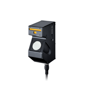
KEYENCE LJ-S8000 Series comes with standard and advanced functions for accurate 3D measurements and inspections. Unlike other solutions requiring external lighting, a staging device, and an encoder, the LJ-S8000 Series line of laser snapshot sensors feature an internal laser lighting source and scanning mechanism. This means there is no requirement for external head rotation. With imaging as fast as 0.2 seconds and repeatability of 0.3 µm, the sensor product is ideal for rapid and precision-based dimensioning, shape, appearance, and other inspection needs.
Contact KEYENCE today for more information about our laser snapshot sensors for the semiconductor industry. Our trained staff will answer all your inquiries regarding integration within your existing manufacturing layout.
Contact us to learn more about how our advanced technology can help take your business to the next level.
Contact Us
Related Downloads
![Automated Measurement and Inspection Examples [Power Semiconductors/Inverters]](/img/asset/AS_111935_L.jpg)
In recent years, the demand for power semiconductors, power modules, and inverters has increased in applications such as electric vehicles. Read about multiple applications putting KEYENCE’s latest laser displacement sensors to good use in production lines of these parts, where quality and safety are both necessary.
Applications
Dimension Measurement
- Thickness and Width Measurement
- Step Height Measurement
- Inner and Outer Diameter Measurement
- Measuring Angles
- Meandering/Edge Measurement
Displacement Measurement
- Positioning and Stroke Length Measurement
- Vibration and Runout Measurement
- Deflection Measurement
- Measuring Eccentricity

