Measurement Sensors
Wafer Notch Detection and Measurement
Semiconductor manufacturing is an intricate process that demands exceptional precision and accuracy, especially since some semiconductive elements are nanometers in size. One of the most important aspects of ensuring the quality and functionality of the wafer is adequate detection and measurement of the wafer notch, which is integral to the whole semiconductor fabrication process.
Get detailed information on our products by downloading our catalog.
View Catalog![Automated Measurement and Inspection Examples [Semiconductors]](/img/asset/AS_119841_L.jpg)
Introduction to Wafer Notch Detection
A wafer notch is a specific indentation on the wafer that serves several different functions in the manufacturing process, such as orientation and alignment of the wafer during production, identification of crystallographic planes, and as a reference point for various automation processes that drive the production.
Thus, detecting and measuring the wafer notch is essential for the entire semiconductor wafer fabrication process. For example, lithography and photoetching demand precise alignment of the wafer itself. Not only that, but adequate wafer notch detection also plays a vital role in maintaining the consistency and quality of the end product and affects its subsequent performance.
Advanced Sensors for Precise Notch Measurement
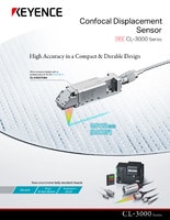
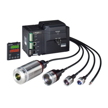
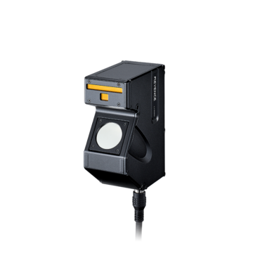
The precision in notch detection and notch measurement largely depends on the sensor technology used for such tasks. The notch is interpreted as a difference in height on the wafer surface, which can be measured with the CL-3000 Series Confocal Laser Sensor. This is also used to check for the wafer setting height inside coating and chemical etching equipment.
The CL-3000 Series is a 1D laser displacement sensor that features an exceptionally high accuracy of 1µm, making it suitable for high-precision measurements and tasks such as precise notch detection. Newer CL sensor heads only contain lenses (all electrical components are contained in an external optical unit).
As a result, this semiconductor sensor can work in ultra-high vacuum and explosive-proof environments. It doesn't introduce electrical noise, and is capable of measuring highly reflective targets (like wafers) thanks to its confocal design.
Integrating Notch Detection in Semiconductor Fabrication
Integrating notch detection into semiconductor fabrication lines includes several key considerations. Namely, the system has to be compatible with the existing fabrication system, its automation protocols and any machinery.
It should also be capable of operating under clean-room conditions, which are typical for semiconductor fabrication. Integration is usually done through software that has real-time data processing capabilities to ensure easy streamlining of the production process while reducing the likelihood of errors.

Enhancing Wafer Alignment with Accurate Notch Detection
Producing microchips is a highly precise and intricate process. Any misalignment of the wafer (including that of the wafer notch) can lead to defects in the etched circuitry and ultimately reduce the yield of usable chips.
Fortunately, introducing adequate notch detection can improve the accuracy of your photolithography stage, during which the circuitry is etched into the silicon wafer. Needless to say, this accuracy is responsible for maintaining the ongoing miniaturization of electronics.
Challenges in Measuring Wafer Notch
Despite the latest technological advancements, wafer notch measurements still present several challenges, especially in high-volume production lines. These mostly include particulate contamination and temperature fluctuations, but the greatest challenge is the reflective property of silicon. Fortunately, the CL-3000—with its multi-wavelength light and sophisticated processing algorithms—solves these issues.
How KEYENCE Measurement Sensors Improve Wafer Notch Detections
KEYENCE is the world’s leading provider of cutting-edge precision measurement sensors and technologies that are widely used in semiconductor manufacturing. If you’re looking to enhance your wafer inspection capabilities, don’t hesitate to contact KEYENCE and inquire about possible integrations of our equipment with your existing production lines.

FAQs
How are Semiconductor Wafers Measured?
Semiconductor wafers are typically measured using precision measurement sensors, such as the CL-3000 from KEYENCE.
What is a Wafer Sensor?
A wafer sensor is a precision measurement device used in semiconductor manufacturing to accurately measure the position and alignment of wafers.
What is Semiconductor WFE?
Semiconductor Wafer Fab Equipment (WFE) is used in the manufacturing of semiconductor wafers, which are used to create microchips and other electronic devices. This equipment includes processes such as photolithography, etching, and deposition.

Related Downloads
![Automated Measurement and Inspection Examples [Power Semiconductors/Inverters]](/img/asset/AS_111935_L.jpg)
In recent years, the demand for power semiconductors, power modules, and inverters has increased in applications such as electric vehicles. Read about multiple applications putting KEYENCE’s latest laser displacement sensors to good use in production lines of these parts, where quality and safety are both necessary.
Applications
Dimension Measurement
- Thickness and Width Measurement
- Step Height Measurement
- Inner and Outer Diameter Measurement
- Measuring Angles
- Meandering/Edge Measurement
Displacement Measurement
- Positioning and Stroke Length Measurement
- Vibration and Runout Measurement
- Deflection Measurement
- Measuring Eccentricity