Measurement Sensors
Semiconductor Wafer Defect Inspection
Manufacturing semiconductor wafers and glass substrates (crucial for LCDs) requires a high degree of precision. The uniform layer thickness of adhesive and resist directly affect product quality. This section introduces coating inspection improvement and adoption examples, as well as useful cases for improving equipment operation and processes requiring high accuracy.
Get detailed information on our products by downloading our catalog.
View Catalog![Automated Measurement and Inspection Examples [Semiconductors]](/img/asset/AS_119841_L.jpg)

Inline 100% Inspection of Wafer Outer Diameters
In semiconductor manufacturing, as many chips as possible are laid out on a wafer to increase chip production. However, if the outer diameter of a wafer is slightly smaller than the specification, the chips positioned along the circumference of the wafer will be defective. In such cases, the wafer cannot yield the designed number of acceptable chips, resulting in lower production.
Conventional offline sample inspection does not eliminate out-of-specification wafers from the process.
The introduction of the High-speed Optical Micrometer LS-9000 Series enables inline 100% wafer diameter inspection before processing.
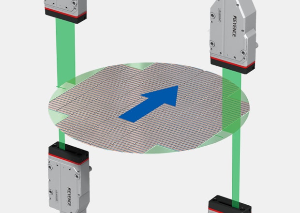
For example, passing a wafer between the LS-9000 Series transmitter and receiver during transferring to the processing equipment enables outer diameter measurements in the order of microns.
With a high-speed measurement processing of 16,000 cycles per second, measurement will not affect the takt time. Instantaneous detection of deviation or inclination of the target during transfer is also possible, allowing for automatic correction before measurement. This ensures stable measurement in the line under various conditions.
Confirmation of Wafer Setting Height Inside Equipment
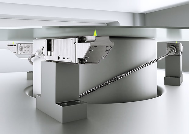
During the mass production of semiconductors, even subtle inclinations or height differences between wafers set in the processing equipment will cause defective processing. The accuracy required for equipment operation is extremely high. To maintain processing quality, measurement and monitoring absolutely must be conducted inside the equipment.
However, installing conventional units is difficult due to a lack of space. Fortunately, KEYENCE’s Confocal Displacement Sensor CL-3000 Series is less constrained by the limited installation space inside the equipment.
Gap Measurement for Slit Coaters
Slit coaters (slit-type coating equipment) discharge the coating fluid from a slit nozzle and coat a uniform layer of fluid on glass substrates, resin substrates, films, or metal foils.
The high-accuracy coating is required for LCD manufacturing processes and Fan-Out Panel Level Packaging (FOPLP) in the semiconductor industry. Even slight variations in the gaps between the slit nozzle and the target on the right or left end directly affect the process, causing coating defects or defective products.
The sensor heads of the Confocal Displacement Sensor CL-3000 Series are extremely compact and lightweight compared to conventional heads. They are also unaffected by heat and electrical noise, so they can be installed inside the equipment even when space is limited, ensuring high accuracy and stable measurement.
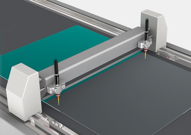
Moreover, the CL-3000 Series can accurately differentiate the top and bottom surfaces of transparent objects with a thickness of 15 µm or more (such as glass substrates, transparent films, and thin layers of transparent materials), allowing for height (distance) measurement.
This enables accurate, simultaneous measurement of the distance from the slit nozzle to the surface of the glass substrate, and of the thickness of the substrate. Maintaining high-accuracy coating is also possible by sending the measurement results to the equipment for height control.
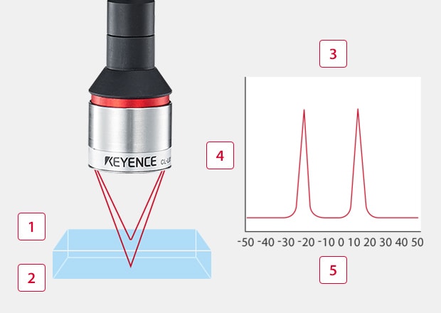
Example of the measurement of transparent objects (using CL-PT010)
-
1Top surface
-
2Bottom surface
-
3Received light waveform
-
4Received light intensity
-
5Height (µm)
Positioning of Glass Substrates
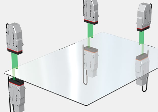
Conventionally, high-accuracy alignment of glass substrates has been done through image processing only. However, pre-alignment was necessary in order to improve processing times while maintaining high accuracy, but pre-alignment was problematic.
The High-speed Optical Micrometer LS-9000 Series provides a mode for measuring transparent targets in addition to a two-level edge detection threshold value setting. This enables stable measurement and positioning without being affected by the edge shape of the thin glass substrate.
How Semiconductor Wafer Defect Inspection Works
Semiconductor wafer manufacturing is a delicate process. Components etched into the wafer are usually in the two-digit nm range (nanometer range) and require highly sensitive quality assurance equipment.
Given the microscale of wafers and the intricate circuitry they contain, even the smallest imperfections can fail the semiconductor chip. As a result, semiconductor inspection equipment must be able to detect tiny variations and a wide variety of defects, including particles, pattern irregularities, and crystallographic disruptions.
Effective semiconductor inspection helps identify these imperfections within the product early in the manufacturing process, thus ensuring the reliability of chips and the overall yield of the entire manufacturing process.
Typically, this is done through high-resolution imaging systems or high-accuracy laser sensors like those manufactured by KEYENCE. These sensors are capable of scanning a wafer surface at high speeds to capture detailed images. Afterwards, those images are further analyzed by specialized software and image processing algorithms, which compare the captured data against standardized blueprints.
For example, the LS-9000 Series high-speed optical micrometer enables 100% inline wafer dimension inspection before processing. Passing the wafer between the receiver and transmitter during operation enables the LS-9000 to measure the outer diameter of the wafer and detect any deviation from the preset values. The system is also used to provide alignment of glass substrates with high-accuracy via image processing alone.
The CL-3000 Series is often used to check for wafer setting height inside coating and chemical etching equipment. At such a microscale, any height deviation will introduce defects into the product, so the accuracy needed for adequate processing has to be extremely high. Additionally, to ensure absolute accuracy, the measurement is often done inside the processing equipment.
CL-3000 confocal laser displacement sensors are also used in slit coating applications to ensure that the applied coating is free of any defects caused by improper gapping between the coater and the target surface. It’s also capable of accurately differentiating between the top and bottom of objects that are transparent, which allows for the height measurement of thin films and other transparent substrates.
Benefits of Wafer Defect Inspection Systems
Implementing KEYENCE high-quality semiconductor defect inspection systems brings several key benefits to semiconductor manufacturing. Effective wafer inspection systems enhance yield by significantly reducing the amount of defective chips proceeding through the production line.
Early defect detection has several benefits. By removing defective products from the production line, KEYENCE products reduce the costs associated with rework later down the production line. This significantly increases the cost-efficiency of the manufacturing process and reduces waste.
Not only that, but the technology can also classify defects by type and severity, allowing manufacturers to decide whether to scrap, rework, or pass the wafer through the next stage of production. Additionally, semiconductors are becoming smaller and their circuitry more complex, so the high accuracy and resolution of the wafer inspection system are becoming more and more critical for production.
Why Choose KEYENCE for Semiconductor Wafer Defect Inspection
KEYENCE is the world’s leading provider of cutting-edge precision technologies and measurement sensors that are often used by numerous industries for industry-specific applications, ranging from manufacturing, medical, food, beverage, and cosmetic industries to industrial process control.
If you’re looking to enhance your wafer inspection capabilities, don’t hesitate to contact KEYENCE and inquire about possible integrations of our equipment with your existing production lines.

Related Products
Related Downloads
-
![Automated Measurement and Inspection Examples [Power Semiconductors/Inverters]](/img/asset/AS_111935_L.jpg)
Automated Measurement and Inspection Examples [Power Semiconductors/Inverters]
In recent years, the demand for power semiconductors, power modules, and inverters has increased in applications such as electric vehicles. Read about multiple applications putting KEYENCE’s latest laser displacement sensors to good use in production lines of these parts, where quality and safety are both necessary.