Measurement Sensors
Dimension Measurement
Displacement Measurement
How to Measure Semiconductors in a Vacuum
A vacuum environment is often used in lab testing as it offers a controlled setting that enhances measurement accuracy. In the context of semiconductor manufacturing, vacuums are necessary for highly advanced measurement and testing requirements.
Let’s discuss the importance of vacuum environments in semiconductor measurement and testing, the challenges these measurements face, and the advantages offered by KEYENCE's measurement equipment for this particular application.
Importance of Vacuum Environments in Semiconductor Measurement
![]()
Confocal Displacement Sensor CL-3000 Series - Measuring Wafer Warpage in a Vacuum
Vacuum environments are important for semiconductor measurement for more than one reason. The primary reason is that vacuums help eliminate contaminants (such as dust and airborne particles) which can interfere with the measurement process.
Why is dust a problem? Many modern electronic components are built on a nm (nanometer) scale, and dust particles can cause measurement inaccuracies. This poses a significant problem for semiconductor manufacturing, which is why measurements are often done in highly sterile, dust-free environments.
There's also a question of moisture, which can lead to measurement interference. Vacuum environments eliminate these contaminants and lead to more accurate and reliable measurement data, which is required for high-precision applications.
Furthermore, vacuum environments are particularly beneficial for surface analysis, and their stable thermal conditions also play a crucial role—they minimize temperature fluctuations that cause the expansion or contraction of all materials, including semiconductors, which affect measurement accuracy.
In short, semiconductor vacuum environments allow you to precisely control experimental conditions, such as pressure, temperature, and gas composition, to ensure repeatable and reliable measurements.
Challenges in Vacuum-based Semiconductor Measurement
Despite its numerous advantages, measuring semiconductors in a vacuum environment isn't without its challenges. One of the primary difficulties is the complexity of the equipment necessary to achieve proper measurement conditions. Achieving a vacuum in an enclosed space isn't that difficult, but doing it without introducing contaminants that might affect the measurement is much more complex.
Creating and maintaining a semiconductor vacuum environment requires some specialized equipment, such as vacuum pumps, chambers, gauges, and valves, whose setup, calibration, and maintenance can be time-consuming. And that’s plenty of complexity without even factoring in the price of equipment.
Furthermore, introducing semiconductor samples for measurement within a semiconductor vacuum chamber without introducing contaminants such as dust is really difficult. Additionally, many of these components are quite sensitive and require special handling tools and equipment to prevent damage.
All of this demands a high level of technical expertise provided by personnel that's well-versed in vacuum technology, measurement technologies and techniques, and the handling of sensitive semiconductor materials.
But the hurdles don't stop there. Vacuum environments don’t eliminate electromagnetic interference or vibrations, which can affect the measurement accuracy and require special shielding and mechanical isolation to mitigate the effects. That's where KEYENCE comes in.
Advantages of Using KEYENCE's CL-3000 Series for Measuring Semiconductors in a Vacuum
![]()
Confocal Displacement Sensor CL-3000 Series - Measuring Stage Tile and Position in a Vacuum
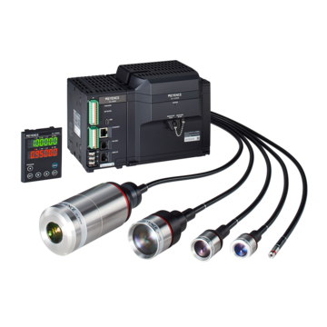
The KEYENCE CL-3000 Series confocal displacement sensors are small, 1D laser displacement sensors that take precision measurements of any surface or material, including dark rubber, thin films, and even the thickness of transparent films. These sensors only have lenses inside the sensor head, which makes them very compact, lightweight, and capable of addressing numerous challenges associated with semiconductor vacuum measurements.
One of those challenges is electromagnetic interference. When sensor heads contain electronic components, interference is common. With the CL-3000 Series, the sensors contain only the lens. Light is generated by a separate optical unit placed outside the measurement location, which eliminates any thermal or electrical noise pickup by the actual sensor head.
Another challenge is outgassing (the process by which gases, vapors, or volatile substances are released from solid or liquid materials when exposed to a vacuum). In the case of semiconductor manufacturing, outgassing commonly occurs when adhesives inside a sensor head are exposed to the vacuum environment. The released substances can contaminate the vacuum environment and impact the performance of sensitive equipment. CL-3000 Series sensors are pre-baked and contain zero organic adhesives, making them ideal for high vacuum environments.
The compact construction of the KEYENCE laser displacement sensors, facilitated by the lack of electronics and adhesives inside the sensor head, also makes them suitable for integration into vacuum chambers with limited space. This ensures durability and longer life expectancy compared to differently designed confocal sensors, with minimal maintenance requirements, which reduces the overall complexity of the entire setup.
Get detailed information on our products by downloading our catalog.
View Catalog

Why Choose KEYENCE?
KEYENCE is the world's leading provider of cutting-edge precision technologies and measurement sensors used by numerous industries for industry-specific applications, ranging from manufacturing, medical, food and beverage, and cosmetic industries to semiconductor, aerospace industries, and industrial process control.
If you're looking to enhance your semiconductor vacuum measurement and other measurement capabilities, don't hesitate to contact KEYENCE and inquire about the possible integrations of our equipment with your existing production lines.
Here are Some of the Most Frequently Asked Questions About Semiconductor Measurement in a Vacuum
What is The Method of Measurement for Vacuum Environments?
As previously stated, vacuum measurement involves specialized equipment and devices to achieve vacuum states, including pressure sensors. Laser displacement sensors are used to measure semiconductors in a vacuum environment due to their non-contact measurement capabilities, which allow for safe and precise measurements of surface profiles and distances.
How do You Measure a Semiconductor?
It depends on the physical property being measured and the sensor used to take the measurement. The CL-3000 Series is often used for measuring wafer setting height inside coating and chemical etching equipment. It’s also used in slit coating applications to ensure that the applied coating is free of any defects caused by improper gapping between the coater and the target surface.
What is Semiconductor Vacuum Measurement?
Semiconductor vacuum measurement refers to the process of testing and evaluating semiconductor devices or elements in a vacuum environment. Vacuums are mostly used in semiconductor manufacturing to perform surface-sensitive measurements without the interference of air and various contaminants.
We’re here to provide you with more details.
Reach out today!

Related Downloads
![Automated Measurement and Inspection Examples [Power Semiconductors/Inverters]](/img/asset/AS_111935_L.jpg)
In recent years, the demand for power semiconductors, power modules, and inverters has increased in applications such as electric vehicles. Read about multiple applications putting KEYENCE’s latest laser displacement sensors to good use in production lines of these parts, where quality and safety are both necessary.
Related Products
Applications
Dimension Measurement
- Thickness and Width Measurement
- Step Height Measurement
- Inner and Outer Diameter Measurement
- Measuring Angles
- Meandering/Edge Measurement
Displacement Measurement
- Positioning and Stroke Length Measurement
- Vibration and Runout Measurement
- Deflection Measurement
- Measuring Eccentricity

