Vision Examples in the LCD/Semiconductor Industry

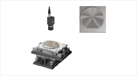
Seating confirmation of a wafer (center coordinates detection)
Detect the center coordinates of a wafer. With conventional machine vision, the edge could not be recognized accurately in some cases due to the influence of the notch or background. As a result, the wafer center was detected incorrectly.
With the XG-X/CV-X Series, a virtual circle can be drawn based on the partial arc of the wafer to allow detecting the center coordinates of the wafer. This ensures accurate confirmation of the seating position. The Trend edge function improves the accuracy of the positioning by increasing the measured points to up to 5,000. It is also possible to count wafers or check inclination simultaneously. An ultra-compact camera is also available, which solves the problem of installation location.
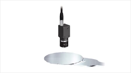
Inspecting the appearance of display devices
Inspect display devices. Conventionally, an area camera was used for appearance inspection of display devices. The inspection was unstable due to frequent lighting unevenness.
Line scan cameras allow inspection over large areas under the same lighting conditions. This significantly improves the stability of appearance inspection of LCD panels that are easily affected by lighting unevenness. In conventional systems, replacing an area camera with a line scan camera required checking compatibility with existing instruments, changing settings, and programming. With the XG-X/CV-X Series, line scan cameras can be used the same way as area cameras. Since the mixed use of area cameras and line scan cameras is also possible, the system can flexibly adapt to changes in the specifications in the future.
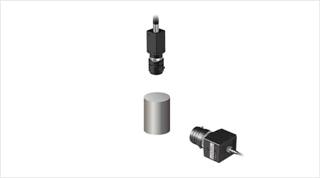
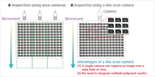
Inspecting the presence/orientation of targets on a tray
To perform inspection over a wide field of view such as inspection for presence/orientation of targets on a tray, you had to divide the inspection range and use multiple area cameras to capture images individually. This increased both takt and cost.
Replacing the area cameras with a line scan camera eliminates the need to divide the inspection range and reduces takt and cost. The need to move the cameras is also eliminated. This allows significant savings of the labor for robot control and changeover work. Since the XG-X/CV-X supports both area cameras and line scan cameras, equipment replacement can be reduced to a minimum.
Inspecting the color of solar cells
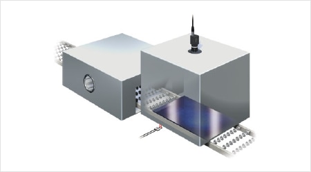
Image processing has been used for color inspection of solar cells. It was difficult to apply lighting evenly, resulting in incorrect detection. Visual inspection was also performed as a countermeasure, but the differentiation criteria varied depending on the personnel and it was difficult to ensure consistent product quality.
Even when the lighting is uneven, Fine Color Processing by the XG-X/CV-X Series allows detection of color changes only, by ignoring brightness information. This effectively prevents the risk of the outflow of defective products and increases the efficiency of the inspection to achieve productivity improvement.
Detecting bad marks on a semiconductor surface
Detecting bad marks on a semiconductor surface. Conventional systems could not differentiate bad marks from stains or marked characters because of the difficulty of light selection. The inspection had to be done visually, costing a lot of labor.
The XG-X/CV-X Series offers Fine Color Processing that allows recognition of subtle color differences. The system can accurately detect bad marks only. This prevents the outflow of defective products and saves labor through automation.
Inspecting for bent IC lead terminals
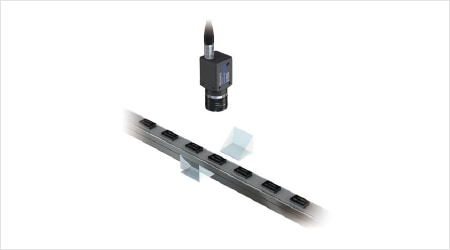
Check for bends in the lead terminals of IC chips. Conventionally, machine vision could not recognize subtle changes so stable detection was difficult. The distance between the reference line at the lead tips and the lead terminal edges had to be calculated individually, which required extra labor.
The XG-X/CV-X Series includes models capable of supporting 21 megapixels and high-speed processing. It can recognize subtle changes that could not be detected with conventional systems. Using the Trend edge stain mode, you can detect bends only by just setting the tolerance without the need to prepare calculation formulas.
Checking broken electrode patterns in solar cells
Check for broken electrode patterns in solar cells. Conventionally, visual inspection was performed. To prevent oversight and ensure stable inspection, it was necessary to increase the number of inspection personnel.
With the XG-X/CV-X series, there are also high resolution cameras with 21 million pixels and high precision inspection is possible. Efficiency can be greatly increased compared to visual inspection. A single unit covers the work of several inspection personnel. Various image enhance filters help improve inspection stability. They ensure reliable detection of defects that may be overlooked in visual inspection.
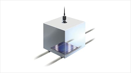
Checking LCD segments
Check the lighting and display of LCD segments. Conventionally, the inspection was done visually. Defective products often passed inspection and labor costs were high.
Image processing can be used for the automation of the display checking of LCD segments. The XG-X/CV-X Series includes a lineup of models capable of high-speed processing. It allows inline inspections and improves production efficiency while reducing labor costs. The inspection can not only check for unlit segments but also compare lighting segments.
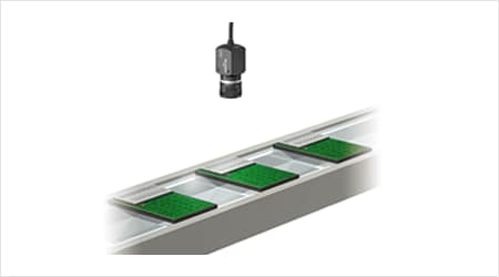
Inspecting BGA ball positions
Check the position of the balls in a BGA (Ball Grid Array) package. Conventionally, a dedicated inspection system was used and visual inspection was performed in the final step. This required time and labor.
The XG-X/CV-X Series can be used easily to check BGA balls and patterns. There is no need to introduce a dedicated inspection system. The versatility is high and it is easy to change models in accordance with inspection targets.

Inspecting the position of wafer notches
Using image processing, detect wafer notches to determine rotation position. Conventional inspection used common 2 megapixel cameras. For the inspection of an entire wafer, the accuracy of the detected position was not satisfactory due to their low resolution.
The XG-X/CV-X Series supports high-pixel cameras with 5 or 21 megapixels, which ensures sufficient accuracy. Using the Profile Defect stain mode enables high-accuracy detection of the concave notch. The inspection is stable even when the position of the wafer changes because Profile Defect stain mode uses an algorithm that detects the point showing the greatest deviation from the reference free-form shape area.
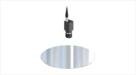
Positioning cells and inspecting for chipping at four corners
Perform positioning of cells and inspection for chipping at four corners simultaneously. Common high-resolution cameras were used. The transmission speed was so slow that it was impossible to improve the operation speed of the production line to the target value.
The XG-X/CV-X Series supports a 21 megapixel camera designed for high-speed processing with a transmission time of 109.9 ms. There is no need to adjust the operation speed to the transmission speed. The double-buffer function further encourages ultra high-speed processing to make the most of the operation speed of the production facility. By using the Trend edge stain function, you can identify defects in the profile extracted from the target and measure the size of chipping simultaneously.
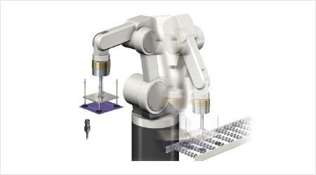
Inspecting collets for foreign particles
Inspect collets for the adhesion of foreign particles. Conventionally, this was checked visually by operators. It took time and was a factor of yield rate reduction.
Use machine vision to check if any foreign particles such as dicing scraps or contamination are adhered on the tip of the collet for picking up chips. This prevents conduction failure or other problems. The XG-X/CV-X Series is capable of high-speed processing so 100% inspection can be achieved without reducing production efficiency. This is also effective for preventing the outflow of defective products and reducing losses from disposal. The facility can be operated at a faster speed, leading to increased yield rates and improved productivity.
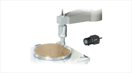
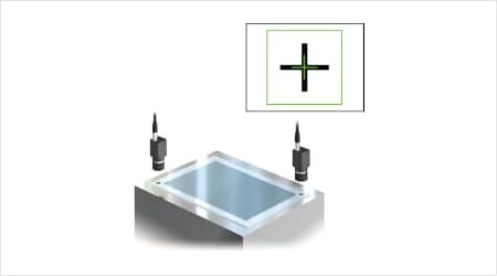
Detecting alignment marks on a glass substrate
Detect alignment marks on glass substrates to perform positioning. Image processing systems have been used for alignment and positioning conventionally, but calibration required a lot of labor. Sometimes defective products were produced due to low accuracy.
The XG-X/CV-X Series offers Auto-calibration to complete calibration automatically. Pattern search is used to detect the positions of alignment marks and then the stage is positioned automatically. This enables high-speed and accurate alignment adjustment to improve takt.
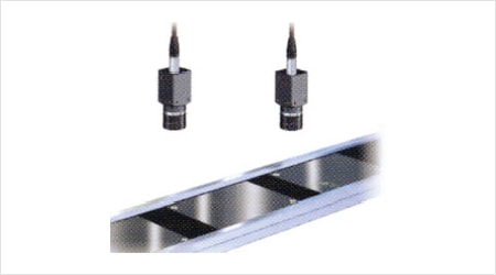
Positioning the orientation flat of a wafer
Set the position of an orientation flat of a wafer. Conventionally, a dedicated system was used to align the angle. It consumed a lot of labor and was a big factor of yield rate reductions due to misalignment.
Using an image processing system to measure the position of the orientation flat, calculate the inclination and adjust the angle can prevent reductions of the yield rate.
Measuring wafer position during handling
Measure the position of a wafer during handling. Conventionally, position was not measured during handling, which caused defective products.
Using an image processing system to accurately measure the position of a wafer before handling can prevent mistakes in subsequent processes.
Checking wafer position in a rack
Check the positions of the wafers inserted in a transfer rack. It was difficult for conventional image processing systems to check the number and positions of the wafers accurately because of the low contrast with the background.
With the XG-X/CV-X Series, packet edges that have low contrast with the background can be identified accurately through the use of the Blur filter, Shading correction and Contrast conversion. This allows accurate detection of the wafer angle.
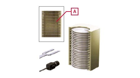
Improperly inserted wafer
Checking the position accuracy of a transfer arm
Confirm the position accuracy of the robot arm that transfers wafers. The position accuracy was not confirmed conventionally. Sometimes the robot arm deviated and broke a wafer.
Using machine vision to constantly confirm the stop position of the robot arm prevents problems. By checking the stop position and dynamic accuracy with machine vision, you can recognize the lowering or deviation of the arm to find the appropriate adjustment timing.
Positioning LCD panels for lamination
Perform positioning of LCD panels for lamination. The lamination of LCD panels requires high accuracy, but conventional machine vision had problems with long calibration times.
The XG-X/CV-X Series offers the Auto-calibration function to reduce labor for calibration and improve production efficiency. Pattern search accurately detects alignment marks and highly-accurate Sub-pixel processing achieves reliable positioning.
Confirming wafer position during transfer
Confirm the positions of wafers during transfer. Conventionally, this was done visually by operators. The judgment varied depending on the operator and it was difficult to ensure consistent product quality.
Using machine vision to confirm the positions of wafers during transfer and keep the position constant ensures consistent product quality. This also reduces the burden on operators and saves labor.
Inspection for breaks and flaws in glass substrates
Inspect glass substrates for flaws or chipping. With conventional image processing systems, it was difficult to find subtle defects due to low resolution and they could not prevent the outflow of defective products.
The XG-X/CV-X Series supports high-resolution cameras with 21 megapixels and offers Profile Defect stain mode to reliably find subtle flaws and other defects in glass substrates.
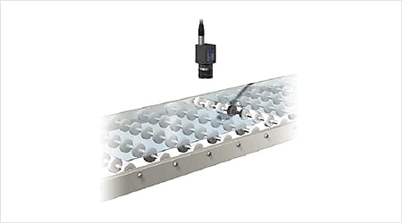
Searching for LCD alignment marks
Search for alignment marks on glass substrates. Conventional detection failed when the alignment marks were not clear.
Utilizing Shape Trax II of the XG-X/CV-X series, it is possible to stably detect unclear alignment marks with high precision. The latest algorithm ensures stable and fast search regardless of defects, inversion, size fluctuation, or brightness change.



![A Technical History of Image Processing Vol.1 [Camera]](/img/asset/AS_46814_L.jpg)
![The Latest Image Processing Applications [Transportation Industry]](/img/asset/AS_71759_L.jpg)

![The Latest Machine Vision Inspections [Food and Medical Industries]](/img/asset/AS_72814_L.jpg)
