Vision Systems
Wafer Notch Detection for Semiconductor and Electronics Industry
For over three decades, KEYENCE has prioritized user experience and reliability, leading the industrial automation industry in innovation, releasing vision systems used across all manufacturing.
The XG-X Series, CV-X Series, and other lines of similar products are precision-based vision system solutions for wafer notch detection and defect inspection in the fabrication of these substrate materials and other intricate electronic parts. From high-resolution cameras and powerful sensors to advanced processors and programming workflow, manufacturers can now make rapid and precision-based quality inspections.

Challenges in Wafer Notch Detection for Semiconductor and Electronics Industry
Detecting Wafer Notches
Detecting wafer notches can be challenging due to their varying shapes, sizes, and orientations. Adaptable detection methods required by different notch styles aren’t available in conventional systems.
Rough Wafer Surfaces
Rough wafer surfaces can reduce the accuracy of optical detection systems. Wafer surfaces can also be contaminated with residue, particles, and other foreign materials, making the notches undetectable.
Transparent Wafers and Unique Coating
Detecting wafer notches with conventional thru-beam sensors requires a bulky transmitter and receiver. These systems have difficulty finding transparent wafers (SiC) and other unique wafer coatings. Plus, thru-beam sensing takes valuable time and mechanical space.
Handling Multiple Notches on a Single Wafer
Latest fabrication process often requires multi-wafer processing, with many systems struggling to handle multiple notches on a single wafer. This is a challenge for older detection systems as they lack the required advanced software and hardware capabilities.

Vision Systems for Wafer Notch Detection for Semiconductor and Electronics Industry
KEYENCE offers a range of wafer notch inspection and detection solutions in semiconductor fabrication of microelectronic devices. Introducing unique wafer coatings and transparent wafers (SiC) limits the operational efficiency of traditional systems like beam array sensors. These old systems can even become a barrier to accurate wafer defect detection as they lack the technologies needed. Depending on the setup and detection goals, KEYENCE has vision and sensor systems for every semiconductor wafer defect inspection, from line scan cameras to inline 3D inspection vision systems for medical device manufacturing.
Line Scan Technology
The Line Scan technology built into the KEYENCE Line Scan Series captures high-resolution 2D images of up to 142,800 lines per second. This technology helps extract defects on fast moving lines that regular inspection cameras can’t detect.
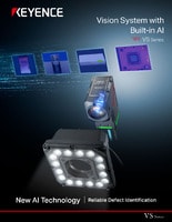
Intuitive Vision System
The CV-X Series is a line of KEYENCE intuitive vision systems that makes advanced and intricate inspections possible for operators of all experience levels via simple clicks and interactive menus.
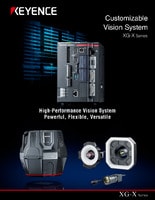
Customizable Vision System
From accurately identifying the wafer’s notch position to carrying out wafer defect detection, KEYENCE customizable vision systems use advanced flowchart style programming and advanced imaging capability to help the advanced user.
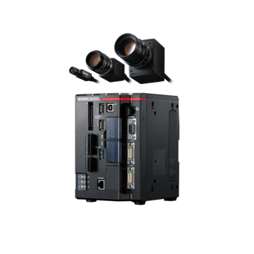
Inline 3D Inspection
KEYENCE inline 3D inspection technology helps handle advanced and intricate processes as wafer notch detection. Make accurate detections with powerful functions, including two cameras within one system, with a field of view up to 60 × 60 mm (2.36″ × 2.36″) and a 9+ megapixel image sensor.
FAQs about Wafer Notch Detection for Semiconductor and Electronics Industry
How Does the KEYENCE XG-X/CV-X Series Improve Wafer Notch Detection Compared to Conventional Systems?
The KEYENCE XG-X/CV-X Series improves wafer notch detection with its high-resolution 3D scanning technology, flowchart style programming, and other advanced features lacking in traditional systems.
Can the Vision Systems Detect and Inspect Wafer Defects Reliably Across Different Positions on the Wafer?
Advanced vision systems like the KEYENCE XG-X/CV-X Series can detect and inspect wafer defects using high-precision features such as high-res cameras and multi-spectral imaging, regardless of the wafer’s notch style.
How Can Wafer Defect Detection Improve Semiconductor Manufacturing Quality and Yield?
Precision-based semiconductor wafer defect inspection helps prevent misalignments or scratches during fabrication processes. Eliminating the large costs of wafer replacements helps manufacturers improve production quality and yield.
What Are the Benefits of Using High-Resolution Cameras for Wafer Notch Inspection?
High-resolution cameras producing high-quality images are significant factors in successful and accurate wafer and wafer’s notches defect detection and positional data.
Can KEYENCE Vision Systems Detect and Inspect Different Types of Wafer Notches Reliably?
Yes, KEYENCE vision systems can reliably detect and inspect all kinds of defects, scratches, cracks, and contamination through high-resolution cameras, powerful processors, advanced-level programming, and quality hardware.
Related Downloads

Industries
- Aerospace
- Automation Equipment/Machine Building
- Automotive
- Commodities
- Defense
- Electric Vehicles
- Electronic Device
- Fabric/Textile
- Food/Beverage Packaging
- Logistics
- Machine Tools
- Marine
- Medical Device Manufacturing
- Mining/Metals
- Paper Manufacturing
- Pharmaceuticals
- Printing
- Semiconductor/Manufacturing Electronics
- Solar
- Tobacco
- Vision-Guided Robotics